
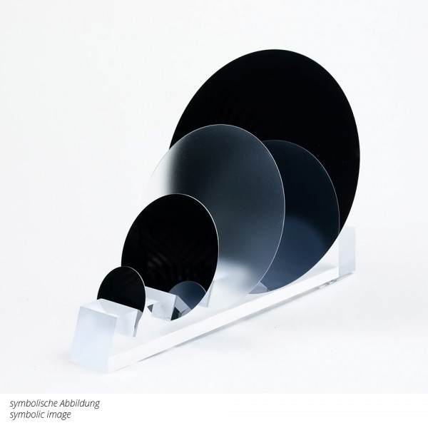
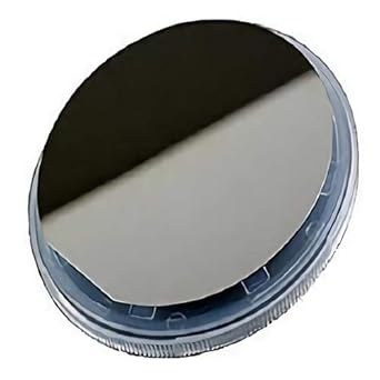
Silizium Wafer
High precision thickness measurement of silicon wafers Capacitive displacement sensors are used for the exact thickness measurement of wafers Two opposing sensors detect the thickness and also determine other parameters such as deflection or sawing marks.

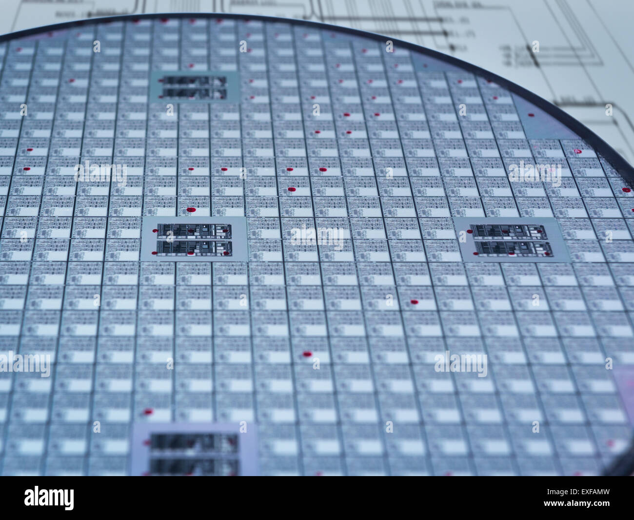
Silizium wafer. A wafer is a thin piece of semiconductor material, normally silicon crystal These wafers are used to fabricate integrated circuits (ICs) and other micro devices Silicon wafers are available in a variety of sizes ranging from 254 mm (1 inch) to 300 mm (118 inches) Top Silicon Wafer Manufacturing Companies in the World. PVD wafer Apollo 300 ECD Wafer Stratus TM P300 Stratus TM P500 1. Silicon wafers and dies are single crystal in semiconductor applications which must withstand high stresses within electronic packages.
Face of the silicon wafer The radiation enters one of the components, then enters the wafer, undergoes total internal reflection, traverses the interface multiply, and exits from another component The IR absorption in the buried layer increases appreciably as a result of multiple passes of radiation through the interface In this. Wafer alignment (by manually approaching the coordinates) inspection point will be acknowledged by the operator by pressing the space key, manual intervention is possible at any time, any magnification and positioning of the stage are possible (with each image an xyposition will be saved as a chip number, coordinate and magnification. Germanium wafers have unique properties that make them a very appealing semiconductor Ge wafers are mechanically strong with a low weight These wafers also posses the ability to be produced with a diameter as large as 300 mm.
The company opened in 1997, producing standard silicon wafers SSP ( single side polished ) test silicon wafers and prime silicon wafers In 1999, Ultrasil started production of DSP (double side polished) Silicon Wafers We shipped our first SOI (Silicon on Insulator) wafer in 01. Topsil silicon wafer solutions are used primarily for energy efficient power components, eg IGBTs and thyristors, and for a number of specialty products targeting detectors, infrared, optical, and communication devices. Wafer Image pv magazine/Harald Schütt The market for silicon wafer, meanwhile, has continued to be defined by the rapid gain in the market share of monocrystalline silicon.
6 inch diameter Silicon Carbide (SiC) Wafers Specifications MSE Supplies offers the best price on the market for high quality SiC wafers and substrates 6 inch diameter Silicon Carbide (SiC) Wafers Specifications Both NType and SemiInsulating Type 4H 6 inch SiC wafers are available. Wafer Image pv magazine/Harald Schütt The market for silicon wafer, meanwhile, has continued to be defined by the rapid gain in the market share of monocrystalline silicon. Chips made out of SOI wafers have the advantage of offering 30% greater speeds and 80% lower power consumption compared to their CMOS counterparts An SOI wafer is made up of 3 basic layers, a device layer, a BOX layer and a Handle layer The BOX layer also called the Buried Oxide layer is trapped between the Device layer and the Handle layer.
This video shows the steps involved in producing a silicon waferSVTI offers courses in IC Layout, PCB Layout, Analog Design, Digital Design, RFIC and Signal. SiliziumWafer VacSol GmbH bietet Standard und kundenspezifische Materialien der Firma TNC Solar Corporation an Dazu gehören mono und multikristalline Wafer für die Herstellung von Solarzellen Die Standardgrößen liegen im Durchmesser bei 610" bzw 125x125mm (Monowafer) und 156x156mm (Multiwafer). The surface of the device wafer is exposed, it might cause particle contamination and contact on the device surface during wafer handling (Fig 1) In contrast, for the edge trimming after bonding, the device wafers must be fully cut, and the cutting amount almost equals to the original thickness of the silicon (Si) wafers.
The company opened in 1997, producing standard silicon wafers SSP ( single side polished ) test silicon wafers and prime silicon wafers In 1999, Ultrasil started production of DSP (double side polished) Silicon Wafers We shipped our first SOI (Silicon on Insulator) wafer in 01. C11 = x 10 11 Pa C12 = 6394 x 10 11 Pa C44 = 7951 x 10 11 Pa Between 150 K and 1000 K the decrease of the Cij with increasing temperature is fairly linear and follows these rates = 94 x 105 K1 7 1 dC = 93 x 105 K1 8 C11 dT 11 = 98 x 105 K1 7 C dT 1 12 dC. Der WaferHersteller Siltronic liefert Zahlen über den Erwartungen, bleibt beim Ausblick aber gedämpft Der Markt setzt bereits auf die nächste Runde im Chipzyklus 1502.
Wafer alignment (by manually approaching the coordinates) inspection point will be acknowledged by the operator by pressing the space key, manual intervention is possible at any time, any magnification and positioning of the stage are possible (with each image an xyposition will be saved as a chip number, coordinate and magnification. Coefficient of Thermal Expansion (CTE) Definition The coefficient of thermal expansion is defined as the fractional increase in the length per unit rise in temperature. Vorrichtung zum Texturieren von Oberflächen von SiliziumScheiben (1), die eine Wanne (3) mit einer Ätzlösung (4) anteilig bestehend aus % bis 55% Wasser, 10% bis 40% Flusssäure mit einer Konzentration von wenigstens 50% und % bis 60% Salpetersäure mit einer Konzentration von wenigstens 65% aufweist, wobei die Vorrichtung dazu eingerichtet ist, die Temperatur der Ätzlösung (4.
Wafer German English translations and synonyms (BEOLINGUS Online dictionary, TU Chemnitz). Most of the wafers used in this study were ground in the ductile mode This is typically the type of surface found on a wafer after completing the grinding process, and thus the extent, and in particular the depth of damage on these wafers has direct influence in the subsequent processing of the wafer. The combination of a fast silicon based switch with a SiC diode – is often termed a “hybrid” solution In recent years Infineon has manufactured several millions of hybrid modules and has seen them installed in various customer products in applications like e g solar and UPS.
Material Category Policy Vishay Intertechnology, Inc hereby certifies that all its products that are identified as RoHSCompliant fulfill the definitions and restrictions defined under Directive 11/65/EU of The European Parliament and of the Council of June 8, 11 on the restriction of the use of certain hazardous substances in electrical and electronic equipment (EEE) recast, unless. SiO 2based SOI wafers can be produced by several methods SIMOX Separation by IMplantation of OXygen – uses an oxygen ion beam implantation process followed by high temperature annealing to create a buried SiO 2 layer;. The reflectivity of a polished silicon wafer is determined from the complex refractive index The data for the above graph is given below As noted above, it is also available in a much more convenient Excel spreadsheet W wavelength a absorption coefficient n real component of refractive index k extinction coefficient refractive index = n ik.
Silicon Wafer Orientation, What you Need to Know Silicon wafers are thin slices of semiconducting material widely used in the production of electronics and micromechanical devices Integrated circuits are often manufactured with a silicon wafer on which a layer of silicon insulator (SOI) is placed SOIs are used to electronically isolate the fine layers of monocrystalline silicon from the rest, and integrated circuits can be manufactured in a much more efficient way than would be used in a. SEMI indicates the bulk, surface, and physical properties required to label silicon wafers as Test Wafers SOI SilicononInsulator (SOI) wafers are silicon wafers having an oxide layer buried below the surface of the crystalline silicon The wafer is a stack of material with silicon on top of oxide on top of silicon. SiliziumWafer {masculine} volume_up 1 electronics SiliziumWafer volume_up silicon wafer Context sentences Context sentences for "Silizium" in English These sentences come from external sources and may not be accurate babla is not responsible for their content.
What is a Silicon Wafer?. Der WaferHersteller Siltronic liefert Zahlen über den Erwartungen, bleibt beim Ausblick aber gedämpft Der Markt setzt bereits auf die nächste Runde im Chipzyklus 1502. What is a Silicon Wafer?.
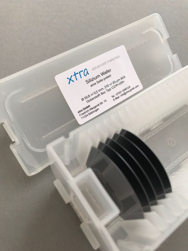
Silizium Wafern Dicke Wafer SVM liefert dicke wafer in allen durchmessern (50mm bis 300mm), mit einer wandstärken spezifikation bis zu und mehr als 2 mm Die oberflächenbehandlung kann geläppt, geätzt oder poliert sein. As technology is rapidly moving forward the reduction of device and chip size is playing an important role to be able to implement as many chips and sensors in smallest space For this reason thickness reduction of the semiconductor wafers is necessary Thin semiconductor wafers (thickness around µm) are. C11 = x 10 11 Pa C12 = 6394 x 10 11 Pa C44 = 7951 x 10 11 Pa Between 150 K and 1000 K the decrease of the Cij with increasing temperature is fairly linear and follows these rates = 94 x 105 K1 7 1 dC = 93 x 105 K1 8 C11 dT 11 = 98 x 105 K1 7 C dT 1 12 dC.
Silicon Wafer Production Czochralski growth of the silicon ingot, wafer slicing, wafer lapping, wafer etching and finally wafer polishing. SEMI indicates the bulk, surface, and physical properties required to label silicon wafers as Test Wafers SOI SilicononInsulator (SOI) wafers are silicon wafers having an oxide layer buried below the surface of the crystalline silicon The wafer is a stack of material with silicon on top of oxide on top of silicon. Tests of silicon wafer Wetting properties & polishing test Microchip production is complicated More than 600 working steps are required to turn the raw material, quartz sand, into a modern processor Most of these steps require the use of special chemicals, for example to clean and etch silicon chips.
The monosilane based polysilicon production process developed by SCHMID Silicon Technology (SST) features highest purity at low cost The material is suitable for the production of multicrystalline, monocrystalline (CZ) and Float Zone (FZ) wafers. Silicon wafers Hyperpure silicon wafers are the basis for almost all semiconductor elements and consequently represent an essential basis for the world’s electronics industry With various diameters, material properties, and surface qualities, Siltronic’s extensive product range covers the global semiconductor industry’s specific requirements. SiliziumWafer VacSol GmbH bietet Standard und kundenspezifische Materialien der Firma TNC Solar Corporation an Dazu gehören mono und multikristalline Wafer für die Herstellung von Solarzellen Die Standardgrößen liegen im Durchmesser bei 610" bzw 125x125mm (Monowafer) und 156x156mm (Multiwafer).
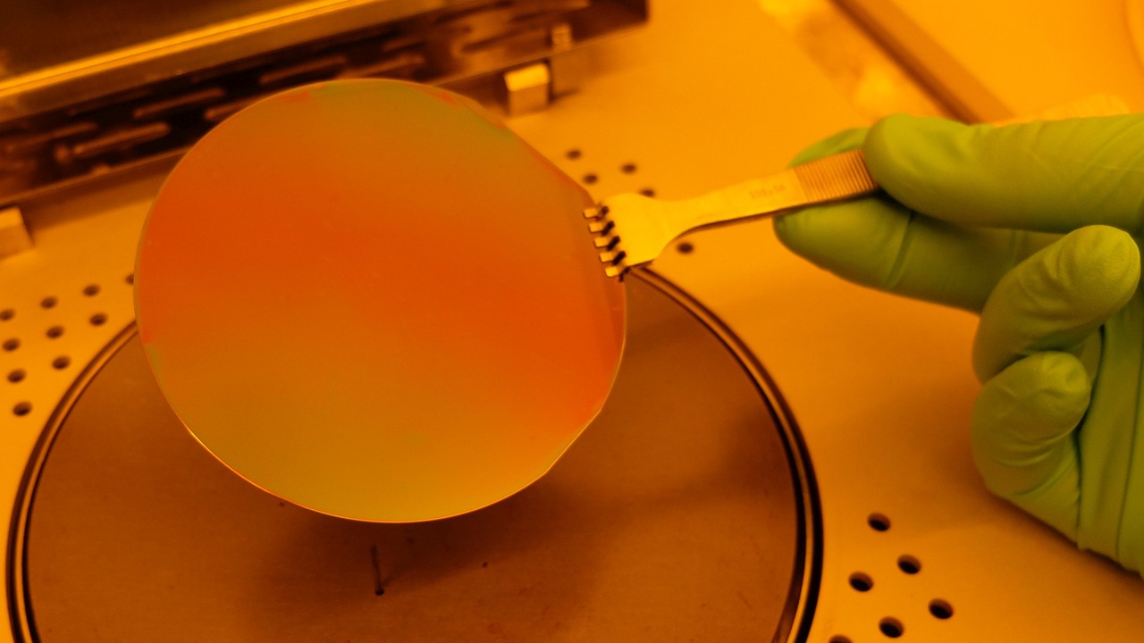
High precision thickness measurement of silicon wafers Capacitive displacement sensors are used for the exact thickness measurement of wafers Two opposing sensors detect the thickness and also determine other parameters such as deflection or sawing marks. I am using Si wafer as the substrate for the growth of 2D materials What makes me feel confused is the composition on the surface In other words, what is on the surface of Si wafer?. The procedural steps of the direct bonding process of wafers any surface is divided into wafer preprocessing, prebonding at room temperature and;.
Silicon Wafer Production Czochralski growth of the silicon ingot, wafer slicing, wafer lapping, wafer etching and finally wafer polishing. Chips made out of SOI wafers have the advantage of offering 30% greater speeds and 80% lower power consumption compared to their CMOS counterparts An SOI wafer is made up of 3 basic layers, a device layer, a BOX layer and a Handle layer The BOX layer also called the Buried Oxide layer is trapped between the Device layer and the Handle layer. What are Silicon Wafers?.
Coefficient of Thermal Expansion (CTE) Definition The coefficient of thermal expansion is defined as the fractional increase in the length per unit rise in temperature. To begin with, we have to acknowledge that semiconductor wafers are made out of silicon an element that makes up almost 30% of the Earth’s crust It is the raw material that constitutes the basic structure of the whole semiconductor chip and is responsible for its optimum functioning. Generally, bow is determined with the wafer in a free, unclamped position (Not to be confused with warp) diameter – the linear distance across a circular silicon wafer which includes the wafer center and excludes any flats or other peripheral fiducial areas edge contour – the cross sectional profile of a wafer edge shaped by grinding or etching Edges may be either rounded or bevelled.
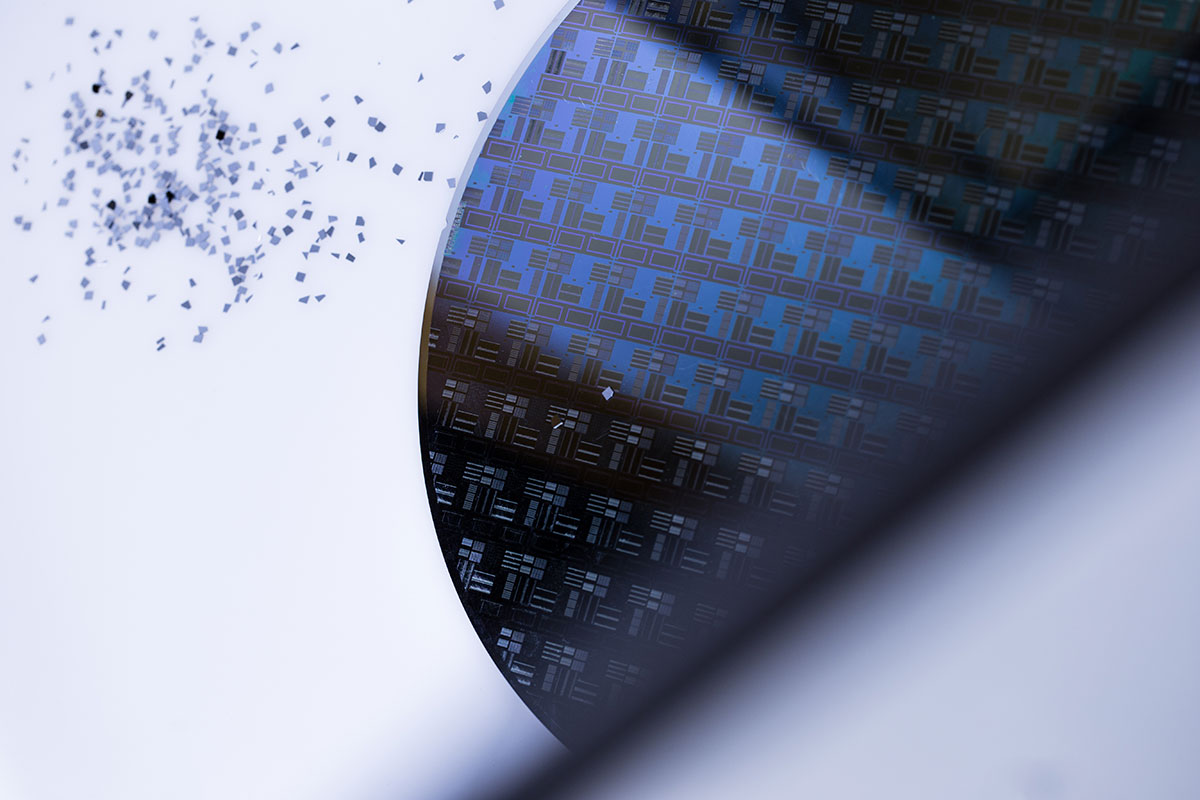
Als Wafer ˈweɪfə(r) (englisch für „dünner Keks“ oder „dünne Brotscheibe“) werden in der Mikroelektronik, Photovoltaik und Mikrosystemtechnik kreisrunde oder quadratische, etwa ein Millimeter dicke Scheiben bezeichnet Sie werden aus ein oder polykristallinen (Halbleiter)Rohlingen, sogenannten Ingots, hergestellt und dienen in der Regel als Substrat (Grundplatte) für. Mit Silizium können zudem grosse WaferScheiben von 30 Zentimetern Durchmesser hergestellt werden, was mit Saphir und SiC nicht möglich ist Weil aber GaN und Silizium verschiedene Materialeigenschaften besitzen, ist es schwierig, die beiden Materialien auf einem Wafer zu vereinen So kann es sein, dass sich bei Erwärmung auf dem Wafer Risse bilden, da sich die Materialien unterschiedlich stark ausdehnen. Wafer bonding – the insulating layer is formed by directly bonding oxidized silicon with a second substrate The majority of the second substrate is subsequently.
We are looking for a Silicon Wafer Manufacturing development engineer (m/f/d) NexWafe’s EpiNex®technology produces highquality, monocrystalline silicon wafers by means of an innovative, continuously operated epitaxial process We have set up a pilot plant in Freiburg to qualify wafers and to prepare for rapid entry into mass production. S H Kim and S Danyluk, “Four Point Probe 9 Resistivity Measurements of Dicing Damage in (100) and (111) Single Crystal Silicon 10 Wafers,” J of Material Science, 25, pp 42–47,1990 CrossRef Google Scholar. Wir beliefern Sie mit Siliziumwafern und anderen Materialien wie Fused Silica Wafer, Borofloat, SOI und Saphirwafer.
A wafer is a thin piece of semiconductor material, normally silicon crystal These wafers are used to fabricate integrated circuits (ICs) and other micro devices Silicon wafers are available in a variety of sizes ranging from 254 mm (1 inch) to 300 mm (118 inches) Top Silicon Wafer Manufacturing Companies in the World. Wafer bonding – the insulating layer is formed by directly bonding oxidized silicon with a second substrate The majority of the second substrate is subsequently. I am using Si wafer as the substrate for the growth of 2D materials What makes me feel confused is the composition on the surface In other words, what is on the surface of Si wafer?.
Annealing at elevated temperatures Even though direct bonding as a wafer bonding technique is able to process nearly all materials, silicon is the most established material up to now Therefore, the bonding process is also referred to as silicon direct bonding or silicon fusion bonding. SiO 2based SOI wafers can be produced by several methods SIMOX Separation by IMplantation of OXygen – uses an oxygen ion beam implantation process followed by high temperature annealing to create a buried SiO 2 layer;. The monosilane based polysilicon production process developed by SCHMID Silicon Technology (SST) features highest purity at low cost The material is suitable for the production of multicrystalline, monocrystalline (CZ) and Float Zone (FZ) wafers.
Tests of silicon wafer Wetting properties & polishing test Microchip production is complicated More than 600 working steps are required to turn the raw material, quartz sand, into a modern processor Most of these steps require the use of special chemicals, for example to clean and etch silicon chips. We are looking for a Silicon Wafer Manufacturing development engineer (m/f/d) NexWafe’s EpiNex®technology produces highquality, monocrystalline silicon wafers by means of an innovative, continuously operated epitaxial process We have set up a pilot plant in Freiburg to qualify wafers and to prepare for rapid entry into mass production. Imbedded abrasive grains – abrasive particles mechanically forced into the surface of the silicon wafer This type of contamination may occur during slicing, lapping, or polishing indent – an edge defect that extends from the front surface to the back surface of the silicon wafer.
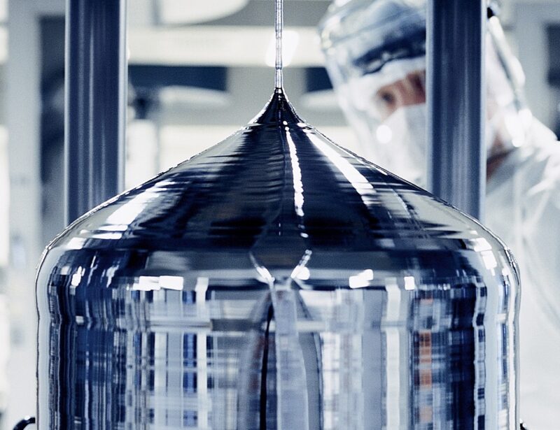
Silicon as it is used in semiconductor manufacturing, is made up of quartz Oxygen which reacts very fast with silicon even at room temperature, and which is present in quartz associated with silicon as silicon dioxide SiO 2, must be removedThis is done just above the melting point of silicon (1414 °C) in furnaces using carbon.
Die Aktuelle Siliziumwafer Situation
:quality(80)/images.vogel.de/vogelonline/bdb/1641100/1641152/original.jpg)
Die Entwicklung Des Silizium Wafers
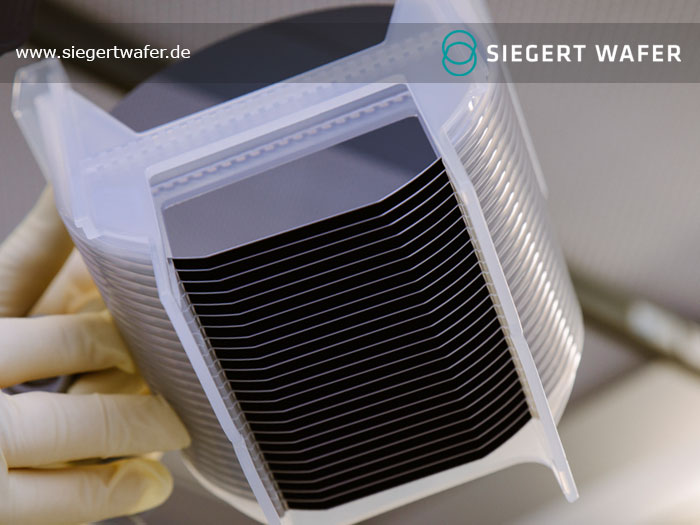
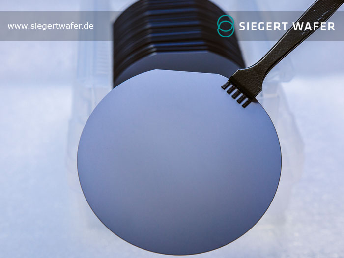
Silizium Wafer Silicon Wafers Siegert Wafer Gmbh
Silizium Wafer のギャラリー
Infineon Chef Galliumnitrid Lost Silizium In Nachster Zukunft Nicht Ab Oiger

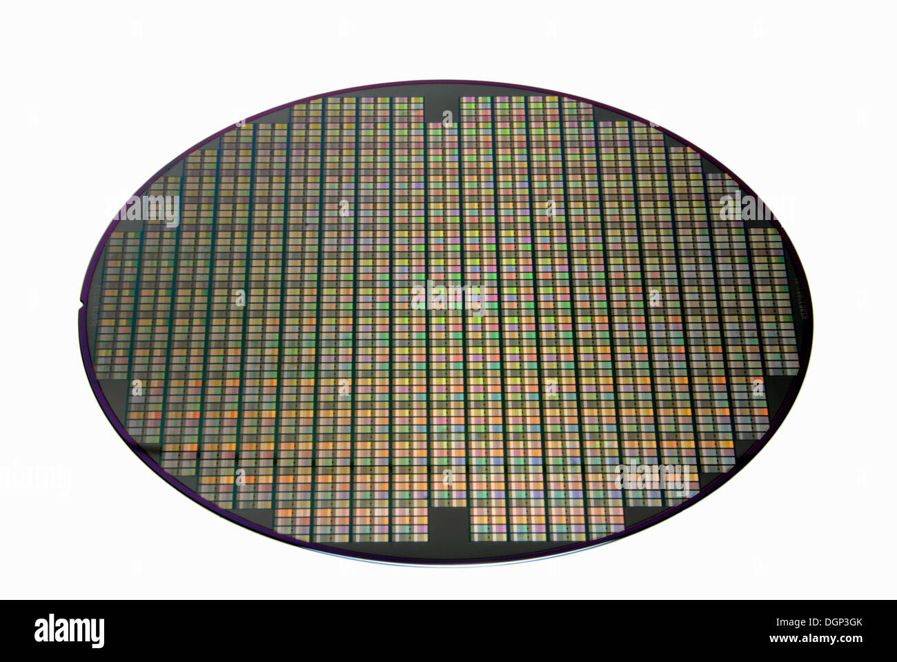
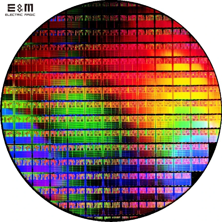
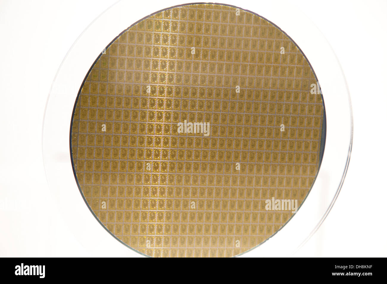
Array Von Cpu Stirbt Auf Einem Silizium Wafer Regenbogen Farben Lizenzfreie Fotos Bilder Und Stock Fotografie Image
1

Universitat Pisa Picosun 1 µf Mm Bei In Silizium Integrierte Mikrokondensatoren Halbleiter Design Elektroniknet

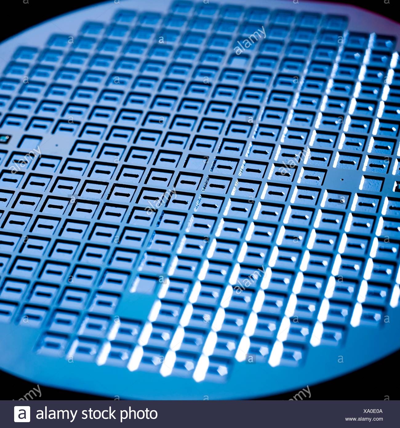
6 8 12 Zoll Wafer Lithographie Chip Silizium Ic Halbleiter Ic

Detail

Detail Von Silizium Wafer Mit Mikrochips Fototapete Fototapeten High Tech Mikrochip Halbleiter Myloview De
Q Tbn And9gcsvtra Yd3hz9k5q4foguz0eru Avnnz2dainias1s Usqp Cau

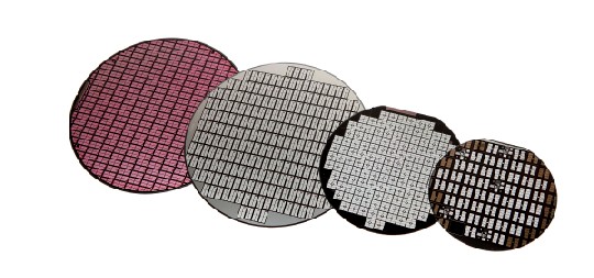
Silizium Wafer Ein Oder Beidseitig Poliert Wie Geschnitten Gelappt Kantenschliff In Vielen Starken Und Grossen
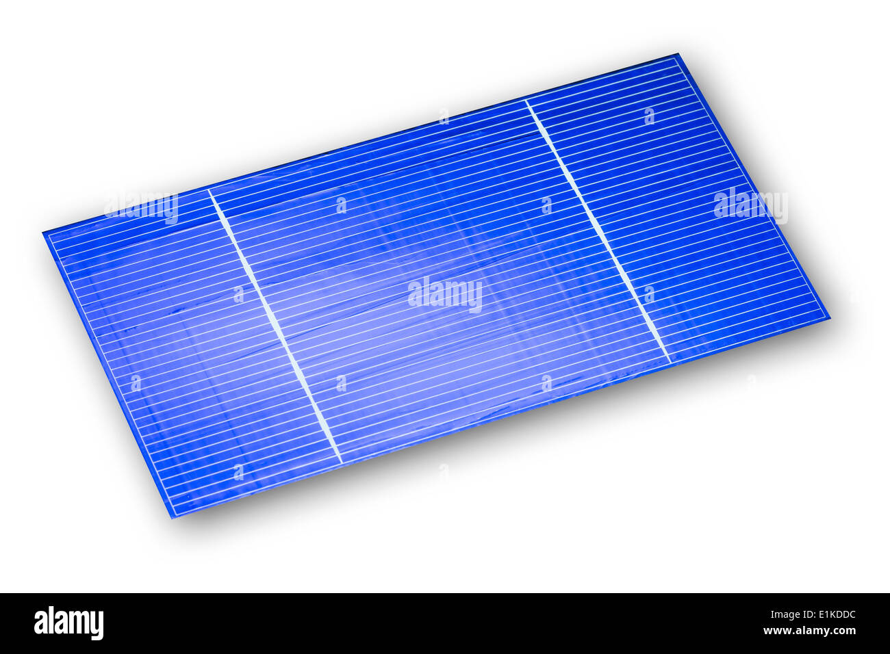
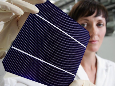
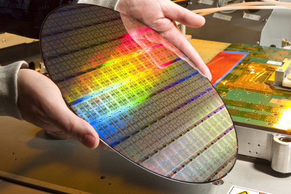
Solarzelle Hochleistungs Solarzelle Aus Einem Monokristallinen Silizium Wafer Hergestellt Das Kontaktgitter Stromschienen Grossere Besteht Aus Stockfotografie Alamy

File Siliziumwafer Stapel Jpg Wikimedia Commons

Prime Klasse 4 Zoll Silizium Wafer Ic Halbleiter Hohe Reinheit Einkristall Poliert Silicon Wafer Elektronenmikroskop Sem Microscope Electronic Microscope Microscopewafer Silicon Aliexpress
Wafer Electronics Wikipedia

Wafer Wikipedia
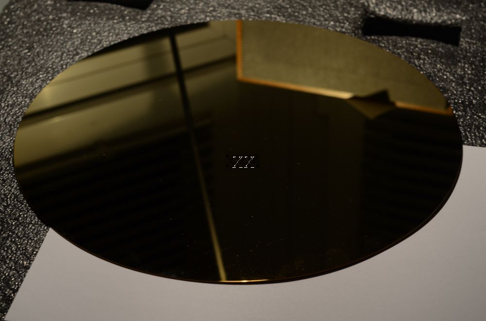
Goldbeschichteter Silizium Wafer Wafer Rem Zubehor Produkte Plano Zubehor Fur Elektronenmikroskopie

Silizium Wafer Verschiedene Ausfuhrungen Und Farben 100 300mm In Sachsen Freiberg Ebay Kleinanzeigen
V Silizium Wafer 12 300mm Mikrocontroller Net

Chip Silizium Wafer 76mm Mit Strukturen Chip Silicone Wafer 3 Inches Ebay

Special Silicon Wafers Amcoss Materials

Silizium Wafer Test Tv Service Portal
Silizium Wafer Nahaufnahme Stockfotografie Alamy

Hintergrundbilder 2560x1600 Px Schaltungen Silizium Wafer 2560x1600 Wallup Hintergrundbilder Wallhere

Detail Von Silizium Wafer Mit Mikrochips Leinwandbilder Bilder High Tech Mikrochip Halbleiter Myloview De

4 Siliziumwafer P Dotiert Einseitig Poliert
Bilderstrecke Zu Regenerative Energie Bosch Ubernimmt Solaranbieter Ersol Bild 1 Von 2 Faz
Supplier Of Silicon Wafers Fused Silica Borofloat And Other Materials Siegert Wafer Gmbh
Silizium Wafer Elektronische Bauteile Halbleiter Platte Stockfotografie Alamy

Silizium Wafer Ein Oder Beidseitig Poliert Wie Geschnitten Gelappt Kantenschliff In Vielen Starken Und Grossen
Silizium Wafer Deutschland Rm Video 660 917 146 In Sd Framepool Stock Footage
Prozessierte Silizium Wafer Cool X
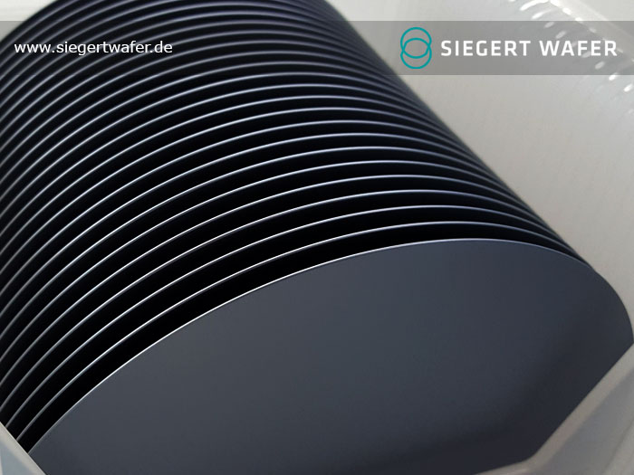
Silizium Wafer Silicon Wafers Siegert Wafer Gmbh
Doppelseitig Polierter Silizium Wafer 101 6 Mm In Erstklassiger Qualitat 10 Amazon De Gewerbe Industrie Wissenschaft
Epi Silizium Wafer Epitaktischer Silizium Wafer Si02 Wafer Si02 Wafer
Vacsol Silizium Wafer
8 Zoll Silizium Wafer Integrierte Schaltung Uncut Geek Spielzeug Ornament Einzigen Kristall Platte Chip Doppel Seite Poliert Si Wafer Ic Integrated Circuit Ic Chipic 8 Aliexpress

Siliziumwafer Mit Einem Muster Auf Surface Multiple Colors Gestapelt Zusammen Von Tweezers Stockfoto Und Mehr Bilder Von Ausrustung Und Gerate Istock

Galliumarsenid Forscher Entwickeln Neues Verfahren Fur Wafer

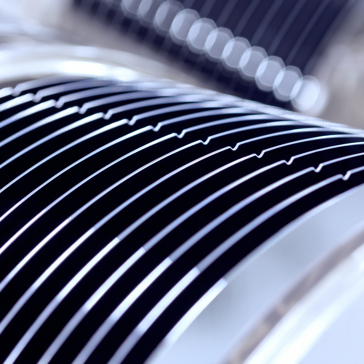
Silizium Wafer Mit Mehreren Identischen Zenith Oszillatoren Watchtime Net
Active Business Company Gmbh Silizium Wafer
Wafer Werden Deutlich Teurer Ram Cpus Und Sensoren Auch
Cpu Lying On Silicon Wafer Stock Photo Panthermedia Stock Agency

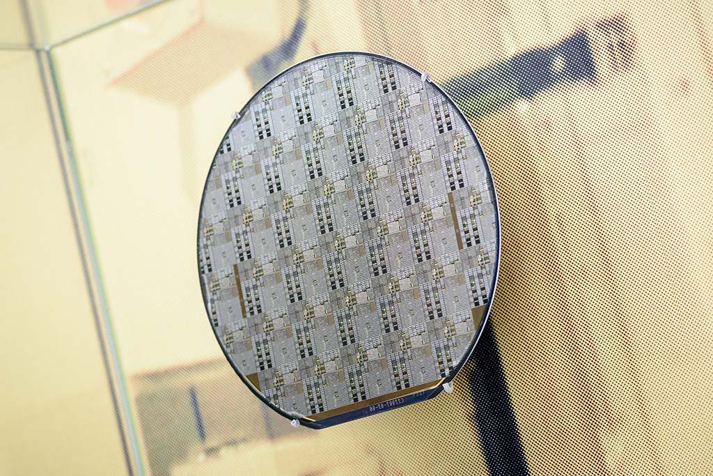
Abb 6 Lichtmikroskopieaufnahme Von Graphen Auf Einem Silizium Wafer Download Scientific Diagram
Mehrstufige Poliermaschine Fur 0mm Silizium Wafer Psg

Silizium Wafer 4 Zoll Doppelseitige Oxidfilm 1000nm 1 Amazon De Gewerbe Industrie Wissenschaft

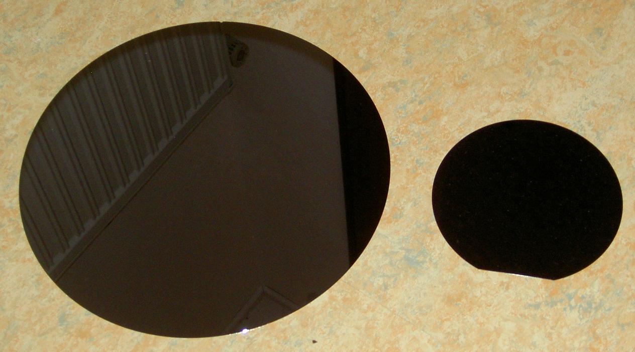
Silizium Wafer

Wafer Wikipedia
Vom Silizium Zum Die Wafer Bearbeitung Im Reinraum Computerbase

Vintage 4 Silizium Wafer Sammler Set Rockwell R6511 Cpu Und Chip Ebay
2 3 4 5 6 8 12 Zoll Silizium Wafer In Fabrik Buy Silicon Wafer Test Poliert Product On Alibaba Com
Xtra Gmbh Siliziumwafer Standard Kundenspezifisch
Fast Efficient Switching Thanks To Hiposwitch Technology Park Berlin Adlershof
Silicon Wafer Cz Wafer Czochralski Silizium Wafer Wafer Shop Produkte Microchemicals Gmbh

Beschichtete Wafer

Die Entwicklung Des Silizium Wafers

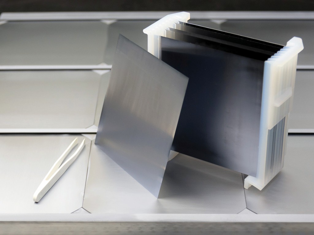
Silizium Wafer In Weisser Plastikhalterbox Auf Einem Tisch Ein Wafer Ist Eine Dunne Scheibe Aus Halbleitermaterial
Supplier Of Silicon Wafers Fused Silica Borofloat And Other Materials Siegert Wafer Gmbh

Kostenloses Silizium Wafer Photos Freeimages Com

Spezial Silizium Wafer Amcoss Materials
Detail Der Silizium Wafer Im Labor Stockfotografie Alamy

Integrierte Schaltungen Ics 8 Zoll Siliziumwafer Vollstandiger Chip Monokristalline Wafer Integrated Circuit Relpcam Com Br

Forschung Grade Substrat Mit Einseitig Poliert Metallisierte Silizium Wafer Si Silizium Oberflache Gold Uberzogene Silber Chrom Nick Flansche Aliexpress
Q Tbn And9gctywn2od Gfo9pp8yezykfc5zxjjznxbk8x4kbosa9drztlcjeq Usqp Cau
Neue Wafer Formate Herausforderung Fur Maschinenbauer Solarserver

Siliziumwafer Detail Von Einem Siliziumwafer Was Verschiedene Farben Stockfoto Und Mehr Bilder Von Ausrustung Und Gerate Istock
Siltronic Perfect Silicon Solutions

Silizium Halbleiter Wafer Scheibe 300mm 12 Mit Strukturen Eine Raritat Ebay

Silizium Carbid Waferherstellung

Beschichtete Wafer

6 Zoll Stark Dotiert Niedrigen Preis Cz Silizium Wafer Fur Halbleiter Buy 6 Zoll Stark Dotiert Niedrigen Preis Cz Silizium Wafer Fur Halbleiter 6 Zoll Stark Dotiert Cz Silizium Wafer Fur Halbleiter Niedrigen
Q Tbn And9gcsvdygheiagvnaelambhcwigirrzrvvtp3yw2ln6 Hwn1pilcjz Usqp Cau

Wafer Wikipedia
Silizium Wafer Computerchip Stockfotografie Alamy

Untersuchung Einer Stichprobe Von Saphir Wafern Unter Dem Mikroskop Im Labor Halbleiter Auf Einem Silizium Wafer Stockfoto Bild Von Labor Wafer
Vom Silizium Zum Die Wafer Bearbeitung Im Reinraum Computerbase

4 Zoll Oxidiert Silizium Wafer Sio2 Wafer Experimentelle Forschung Sonder Oxidation Blatt Wafer Silicon Sheet Silicone Aliexpress
Die Revolution Der Siliziumwafer Ingenieur De

Forschung Silicon Chip Wafer Cmos Bild Sensor Chip Wafer Silizium Wafer Monocrystallin 8 Zoll Integrierte Schaltkreise Aliexpress
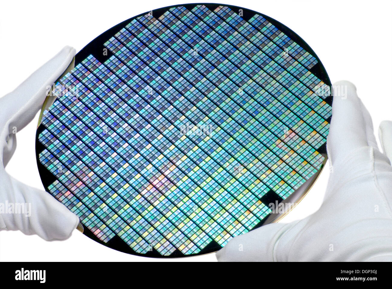
Behandschuhten Hande Halten Einen Silizium Wafer Elektronisches Bauelement Halbleiter Platte Stockfotografie Alamy
Wafer Si Wafer Silicon Offer Request Production

6 Silizium Wafer Performance Semi R4000 Mips Cpu Wafer Mit Versand Fall Ebay

Halbleiter Silizium Wafer Ring Auf Der Maschine Stockfoto Jetzt Bearbeiten
Silizium Wafer Mit Orientierung Typ P Wafer Rem Zubehor Produkte Plano Zubehor Fur Elektronenmikroskopie

Siliziumwafer Mit Einem Muster Auf Der Oberflache Multiple Colors Zusammen Gestapelt Stockfoto Und Mehr Bilder Von Ausrustung Und Gerate Istock

Historische 1 5 Silizium Wafer Vintage 1960s Dtl C261 Fch131 Von Mullard Der Uk Ebay
V Silizium Wafer 12 300mm Mikrocontroller Net

1 Stuck 8 0 Mm Silizium Wafer Ca 0 8 0 9 Mm Dick Matt Spiegelglanzend Eur 4 50 Picclick De

Cmos Silizium Wafer 12 Zoll Wafer Komplette Chip Ic Chip 12 Zoll Photolithographie Wafer 12 Zoll Schaltung Chip Integrierte Schaltkreise Aliexpress
Nano Tec Vergoldete Silizium Wafers Und Chips Fur Mikroskopie Afm Biotechnologie Und Nanotechnologie Anwendungen

Membranpumpen Helfen Bei Der Reinigung Von Silizium Wafern Mit Uberkritischem Kohlenstoffdioxid Chemanager
Wafer Wikipedia

Super Silizium Archiv
Finden Sie Hohe Qualitat Silizium Wafer Carrier Hersteller Und Silizium Wafer Carrier Auf Alibaba Com

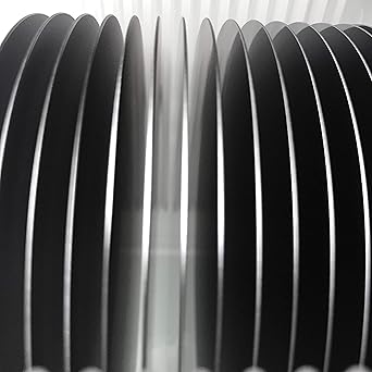
Siliziumwafer

Stuck 8 0 Mm Silizium Wafer Ca 0 8 0 9 Mm Spiegelglanzend Inkl Box Eur 10 00 Picclick De
Silizium Wafer Herstellung Stockfotos Und Bilder Kaufen Alamy

Silicium Wafers Led Paffrath Gmbh High Tech Materials
E4rtrxe8da9scm
Silizium Wafer Silicon Wafers Siegert Wafer Gmbh

Silizium Wafer Stockfotos Freeimages Com

Damasko Atzt Seine Spiralen Aus Einem Silizium Wafer Watchtime Net

Graphene Supermarket 2 Research Materials 4 Silicon Silicon Dioxide Wafers Si Sio2 285nm P Type Wafers Silicon Silicon Dioxide Wafer 4 Diameter P Type


