
Note 4 Datenblatt
Note 1 Pulse test with PW=300μs, 1% duty cycle Note 2 Mounted on FR4 PCB with 16mm x 16mm Cu pad area Note 3 Free air, mounted on recommned pad Note 4 Measured at 1 MHz and Applied V R =40 Volts Document Number DS_D Version B1812 Part no with suffix "H" means AECQ101 qualified 600 405 250 10 500 60 180 140 84 78 TPMR10G.

Note 4 datenblatt. Note 1 voltage accuracy note 2 line regulation note 3 load regulation note 4 average efficency min note 5 trh70a1 12v 580a 1% ±2% ±1% ±4% % trh70a150 1%15v 465a ±2% ±1% ±3% % trh70a180 18v 390a 1% ±2% ±1% ±2% % trh70a190 19v 370a 1% ±2% ±1% ±2% %. Samsung Galaxy Note 4 Datenblatt Fakten zum Galaxy Note 4 im Überblick Erscheinungstermin Oktober 14 Einführungspreis zum Marktstart 769 Euro Insgesamt ist das Samsung Galaxy Note 4 uneingeschränkt empfehlenswert sofern die Größe den ein oder anderen nicht abschreckt Denn mit seinem 5,7 Zoll Quad HD Display passt das Phablet. (Note E) 25°C 125°C 08 1 12 14 16 18 2 22 0 25 50 75 100 125 150 175 On nce Temperature (°C) Figure 4 OnResistance vs Junction Temperature (Note E) V GS =45V I D =A V GS =10V D =A 5 10 15 25 30 35 2 4 6 8 10 R) (m W) V GS (Volts) Figure 5 OnResistance vs GateSource Voltage (Note E) °C 125°C V DS =5V V GS =45V V GS.
In IEC ) without any performance degradation Additionally, each TVS can safely dissipate a 50A 8/μs surge event as defined in IEC 2nd edition Note This package image is for example and reference only for detail package drawing, please refer to the package section in this datasheet 1 2. (see note 4) Mechanical 1,000,000 operations min Electrical 500,000 operations min for a resistive load of 3 A at 250 VAC (see note 5) Operating speed 005 to 05 m/s Operating frequency 30 operations/minute max Rated frequency 50/60 Hz Contact gap 2 x 2 mm min Direct opening force (see note 6) 60 N min (EN). Note (1) Also available in tubes, do not put T on the end B C E A C NC 1 2 3 6 5 4 i ORDERING INFORMATION CN Y 1 7 # X 0 # # T PART NUMBER CTR BIN PACKAGE OPTION TAPE AND REEL AGENCY CERTIFIED/PACKAGE CTR (%) UL, cUL, BSI, FIMKO 40 to 80 63 to 125 100 to 0 160 to 3.
(Note 4) Max Reverse Leakage Current VZ (mV/k) @ IZT = 2 mA C (pF) @ VR =0, f = 1 MHz I R @ V Min Nom MaxA Volts Min BZX84B27LT1G T27 265 27 275 80 005 1 214 253 70 *Includes SZprefix devices where applicable BZX84BxxxLT1G, BZX84CxxxLT1G Series, SZBZX84BxxxLT1G, SZBZX84CxxxLT1G Series. Input Voltage Range with Internal LDO (Note 4, Note 5) PV IN, V IN 60 16 V Supply Voltage Range (Note 2) V CC 45 55 Continuous Output Current Range I O 0 4 A Operating Junction Temperature T J40 125 °C Page 7 Rev 11, Jun 12, Patent Protected US 9,729,059 B1;. Note 2Surface Mounted on FR4 Board,t.
(Note 6) Symbol Parameter Rating Unit θ JA Junction to Ambient SO8EP 45 °C/W θ JC Junction to Case SO8EP 5 °C/W Note 6 Test condition for SO8EP Device mounted on FR4 substrate, fourlayer PC board, 2oz copper, with minimum recommended pad layout Recommended Operating Conditions (Note 7) (At T A = 25°C, unless otherwise specified). (Note 1) 30A VGS Gatesource VoltageV PD Total Power Dissipation 125 W R JA Thermal Resistance Junction to Ambient (Note2) 100 /W TJ Operating Junction Temperature 55 to 150 TSTG Storage Temperature 55 to 150 Internal Block Diagram omponents 736 Marilla Street Chatsworth ˘ ˇˆ ˙ ˝ ˘ ˇˆ Revision A wwwmccsemicom 1 of 4. (Note 4) Part Number Case Packaging BSS127SSN7 SC59 3000/Tape & Reel BSS127S7 SOT23 3000/Tape & Reel Notes 1 No purposely added lead Fully EU Directive 02/95/EC (RoHS) & 11/65/EU (RoHS 2) compliant Figure 4 OnResistance Variation with Temperature R, 50 D R A I NS O U R E O NR E S I S T A N C E (N o r m a l i z e d) D S (O N.
24 17 — V Enable High, (Note 2) — 15 08 Enable Low, (Note 2) Enable Input Capacitance —— 1 — pFNote 3 Switch Resistance RDS(ON) —80 1 mΩ IOUT = 500 mA Current Limit Factor — 184 230 276 V IOUT = 100 mA to 1A, V OUT = 1V to 4V, (Note 4) 161 230 299 IOUT = 500 mA to 15A, VOUT = 1V to 4V, (Note 4) Output Leakage Current. IIL Logic “0” input current VINPUT= L (Note 4) nA IIH Logic “1” input current VINPUT= H (Note 4) nA IS31FL3741 Integrated Silicon Solution, Inc – wwwissicom 6 Rev 0B, 09/06/17 DIGITAL INPUT SWITCHING CHARACTERISTICS (NOTE 3) Symbol Parameter Fast Mode Fast Mode Plus. (Note 2) Note 4 For the LT3092, dropout is specified as the minimum inputtooutput voltage differential required supplying a given output current Note 5 Adding a small capacitor across the reference current resistor lowers output noise Adding this capacitor bypasses the resistor shot noise.
Note The data of D1 is send by MCU,and D2, D3, D4 through pixel internal reshaping amplification to transmit Composition of 24bit data G7 G6 G5 G4 G3 G2 G1 G0 R7 R6 R5 R4 R3 R2 R1 R0 B6 B5 B4 B2 B1 B0 Note Follow the order of GRB to sent data and the high bit sent at first Typical application circuit. Note The Communicationstype CPU Unit has 6 inputs and 3 outputs Expansion I/O Units 1 Number of I/O points 8 4 inputs and 4 outputs 2 Unit version classifier E1 Can connect to V2 CPU Units (See note) 3 Input type A AC input D DC input 4 Output type R Relay T Transistor Note Use a ZEN8E @@ /4E @ to connect to preV1 and V1 CPU. ToCase (Note F) 0 2 4 6 8 10 0 5 010 15 25 30 V GS s) Q g (nC) Figure 7 GateCharge Characteristics 500 1000 1500 00 2500D 3000 5 10 15 pF) V DS (Volts) Figure 8 Capacitance Characteristics C iss 001 01 1 10 1E05 0001 001 01 1 10 100 Z q JC on e Pulse Width (s).
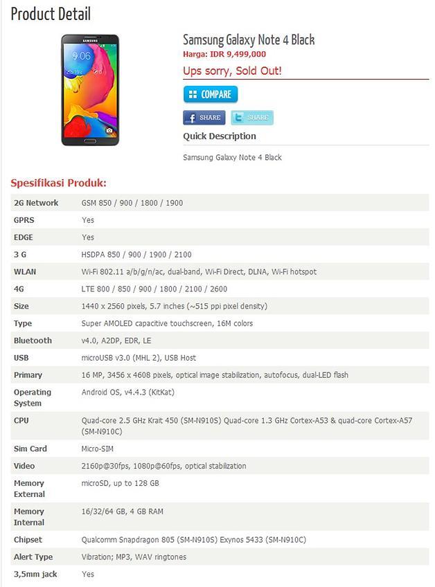
Maximum Output Current IOUT V V 3 3 A0 — m 0 —2 IN, 12V VOUT (Note 4) 375 — mA 50V VIN, 12V VOUT (Note 4) 150 — mA 42V VIN, 24V VOUT (Note 4) Feedback Voltage V FB 1190 1227 1264 V VFB Accuracy 3 — 3 % Feedback Input Bias Current I VFB — 0025 — µA No Load Input Current IIN0 — 250 — µA Device switching, no load,. Fiche technique Samsung Galaxy Note 4 Digne successeur du Note 3, le Samsung Galaxy Note 4 est équipé d'un écran de 5,7 pouces Quad HD Embarquant un processeur Snapdragon 805 quatre coeurs. Samsung Galaxy Note 4 Android smartphone Announced Sep 14 Features 57″ display, Snapdragon 805 chipset, 16 MP primary camera, 37 MP front camera, 32 mAh battery, 32 GB storage, 3 GB RAM.
By 10/1000us Test Waveform(Fig4) (Note 1), (Note 2)Stacked Die Parts (Note 5) P PPM 800 W Power Dissipation on Infinite Heat Sink at T L =50OC P D 50 W Peak Forward Surge Current, ms Single Half Sine Wave (Note 3) I FSM 100 A Maximum Instantaneous Forward Voltage at 50A for Unidirectional Only (Note 4) V F 35/50 Operating Temperature. * The amount of available storage and RAM is less than the indicated memory, as the operating system and preinstalled software are stored in the device Samsung HMX, 108MP, 08μm, 1/133″, f/169 aperture, FOV °, 14μm 4in1 Super Pixel, OIS 12MP portrait camera, 14 μm, ƒ/, 2x optical. Note 4 Logiclow voltages are specified at a sink current of 4mA Note 5 To guarantee a presence pulse under low voltage parasite power conditions, VILMAX may have to be reduced to as low as 05V Note 6 Logichigh voltages are specified at a source current of 1mA.
VHYS (Note 2) 01 × VCC V LowLevel Output Voltage at 4mA Sink Current VOL (Note 7) 04 V Output Fall Time from VIH(MIN) to VIL(MAX) with a Bus Capacitance from 10pF to 400pF tOF (Note 2) 180 ns Input Current with an Input Voltage Between 01VCCmax and 09VCCmax II (Note 2) 1 1 µA Electrical Characteristics wwwmaximintegratedcom Maxim. VOL (Note 4) 04 V Output Fall Time from VIH(MIN)to VIL(MAX) with a Bus Capacitance from 10pF to 400pF tOF (Note 3) 30 ns Pulse Width of Spikes that are Suppressed by the Input Filter tSP (Note 3) 50 ns Input Current with an Input Voltage Between 01VCCmaxand 09VCCmax II (Note 3,Note 5) 1 1 µA Input Capacitance CI (Note 3) 10 pF. TS SetUp Time 400 — — ps Note 4 tH Hold Time 400 — — ps Note 4 tJITTER Additive Phase Jitter, RMS — 80 — fs 628 MHz @ 33V, Integration range 12 kHz to MHz tr/tf Output Rise/Fall Times (% to 80%) 60 110 190 ps At Full Output Swing — Duty Cycle 47 — 53 % Differential I/O Note 1 Highfrequency AC parameters are.
4V = 4 63V = 6 10V = Z 16V = Y 25V = 3 50V = 5 100V = 1 0V = 2 500V = 7 NOTE Contact factory for availability of Termination and Tolerance Options for Specific Part Numbers Contact factory for nonspecified capacitance values X7R formulations are called “temperature stable” ceramics and fall into EIA Class II materials X7R is the. (Note 4) VCC21 100 360 450 490 µA NOTES 3 Any voltage between VCC and GND 4 For dualsupply systems theoretical worst case (VI = 24V, VCC = 55V) specification is 18mA DC Electrical Specifications (Continued) PARAMETER SYMBOL TEST CONDITIONS VCC (V) 25oC 40oC TO 85oC 55oC TO 125oC. TS SetUp Time 400 — — ps Note 4 tH Hold Time 400 — — ps Note 4 tJITTER Additive Phase Jitter, RMS — 80 — fs 628 MHz @ 33V, Integration range 12 kHz to MHz tr/tf Output Rise/Fall Times (% to 80%) 60 110 190 ps At Full Output Swing — Duty Cycle 47 — 53 % Differential I/O Note 1 Highfrequency AC parameters are.
Input Voltage Range with Internal LDO (Note 4, Note 5) PV IN, V IN 60 16 V Supply Voltage Range (Note 2) V CC 45 55 Continuous Output Current Range I O 0 4 A Operating Junction Temperature T J40 125 °C Page 7 Rev 11, Jun 12, Patent Protected US 9,729,059 B1;. 4 3 151±±024 see note 5 (2) pl ±6004±024 see note 5 (2) pl see note 6 see note 7 1816±±015 see note 6 see note 6 white ink dot see note 4 (4) pl 1 3 6 2 4 a/r see notes 5 & 6 (4) pl 1 4 3 readable marking 2 pin protrusion ref seating plane (4) pl 6. See note4 notes 3 indicated holes are unplated 5 this product meets european union directives and other country regulations as described in gs47 0004 2 for plating performance refer drawing contact copper alloy 1 material body lcp ul94v0 7 a symbol will be next to any dimension, view, or note which has been modified.
The Samsung Galaxy Note 4 is an Android smartphone developed and produced by Samsung ElectronicsThe Galaxy Note 4 was unveiled during a Samsung press conference at IFA Berlin on 3 September 14 and was released globally in October 14 It is the successor to the Samsung Galaxy Note 3Its subsequent model, the Samsung Galaxy Note 5, was unveiled on 13 August 15. Maximum Output Current IOUT V V 3 3 A0 — m 0 —2 IN, 12V VOUT (Note 4) 375 — mA 50V VIN, 12V VOUT (Note 4) 150 — mA 42V VIN, 24V VOUT (Note 4) Feedback Voltage V FB 1190 1227 1264 V VFB Accuracy 3 — 3 % Feedback Input Bias Current I VFB — 0025 — µA No Load Input Current IIN0 — 250 — µA Device switching, no load,. (Note 4) Part Number Marking Reel Size (inches) Tape Width (mm) Quantity Per Reel FMMT411TD 411 7 8 500 FMMT411TA 411 7 8 3000 Notes 1 No purposely added lead Fully EU Directive 02/95/EC (RoHS), 11/65/EU (RoHS 2) & 15/863/EU (RoHS 3) compliant 2.
Input Bias Current IVp(E/A) 0 4 µA Sink Current Isink(E/A) 04 085 12 mA Source Current Isource(E/A) 4 75 11 mA Slew Rate SR Note 4 7 12 V/µs GainBandwidth Product GBWP Note 4 30 40 MHz DC Gain Gain Note 4 100 110 1 dB Maximum Output Voltage Vmax(E/A) 17 2 23 V. (Note E) 25°C 125°C 08 1 12 14 16 18 2 22 0 25 50 75 100 125 150 175 On nce Temperature (°C) Figure 4 OnResistance vs Junction Temperature (Note E) V GS =45V I D =A V GS =10V D =A 5 10 15 25 30 35 2 4 6 8 10 R) (m W) V GS (Volts) Figure 5 OnResistance vs GateSource Voltage (Note E) °C 125°C V DS =5V V GS =45V V GS. Note 2Surface Mounted on FR4 Board,t.
Input Voltage Range with Internal LDO (Note 4, Note 5) PV IN, V IN 60 16 V Supply Voltage Range (Note 2) V CC 45 55 Continuous Output Current Range I O 0 4 A Operating Junction Temperature T J40 125 °C Page 7 Rev 11, Jun 12, Patent Protected US 9,729,059 B1;. 1s(Note 4) 2s2p(Note 5) SOP28 Junction to Ambient θ JA 1369 6 °C/W Junction to Top Characterization Parameter(Note 3) Ψ JT 19 15 °C/W (Note 2) Based on JESD512A(StillAir) (Note 3) The thermal characterization parameter to report the difference between junction temperature and the temperature at the top center of the outside. 64 ~ 75V 156~ 18V 175~ 21V 28~ 33V 35g;280psc/108Kg/094CUFT 42A (12/24VDC) FUNCTION EMC EMISSION Parameter Standard Test Level / Note EMC IMMUNITY SAFETY & EMC Conducted EN Radiated EN Parameter Standard Test Level / Note Surge Level 2, 1KV/LineLine, criteriaA SAFETY STANDARD EN(LVD) Radiated EFT / Burst Conducted.
Note The Communicationstype CPU Unit has 6 inputs and 3 outputs Expansion I/O Units 1 Number of I/O points 8 4 inputs and 4 outputs 2 Unit version classifier E1 Can connect to V2 CPU Units (See note) 3 Input type A AC input D DC input 4 Output type R Relay T Transistor Note Use a ZEN8E @@ /4E @ to connect to preV1 and V1 CPU. In IEC ) without any performance degradation Additionally, each TVS can safely dissipate a 50A 8/μs surge event as defined in IEC 2nd edition Note This package image is for example and reference only for detail package drawing, please refer to the package section in this datasheet 1 2. Lees hier alles over de Samsung Galaxy Note 4, de nieuwe en snelle phablet van Samsung Check de Galaxy Note 4 review, prijzen, specificaties en video's.
SmartFusion2 SoC FPGA Architecture SmartFusion2 SoC FPGAs offer 5K150K LEs with a 166MHz ARM® Cortex™M3 processor, including ETM and Instruction Cache with onchip eSRAM & eNVM and a complete Microcontroller Subsystem with extensive peripherals including CAN, TSE, USBArchitecture highlights include. Hier finden Sie alle technischen Daten im Datenblatt zu Samsung Galaxy Note 4 Sie finden zum Galaxy Note 4 von Samsung unter anderem Specs zum Preis, ReleaseTermin, Betriebssystem, Gehäuse. Only(Note 4) V F 35/50 V Operating Temperature Range T J65 to 150 °C Storage Temperature Range T STG65 to 175 °C Typical Thermal Resistance Junction to Lead R ƟJL 15 °C/W Typical Thermal Resistance Junction to Ambient R ƟJA 75 °C/W Notes 1 Nonrepetitive current pulse , per Fig 4 and derated above T J.
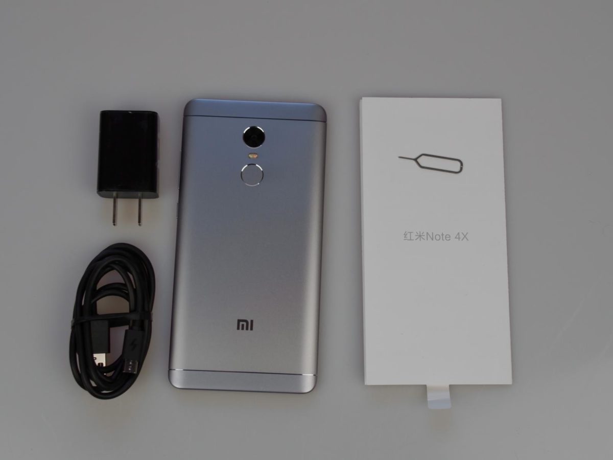
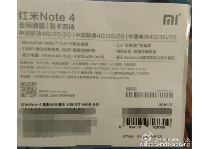
Hier finden Sie alle technischen Daten im Datenblatt zu Xiaomi Redmi Note 4 Sie finden zum Redmi Note 4 von Xiaomi unter anderem Specs zum Preis, ReleaseTermin, Betriebssystem, Gehäuse, Display. Note 4 Logiclow voltages are specified at a sink current of 4mA Note 5 To guarantee a presence pulse under low voltage parasite power conditions, VILMAX may have to be reduced to as low as 05V Note 6 Logichigh voltages are specified at a source current of 1mA. Power Dissipation 175Pd (Note 2) 375 (Note 3) W Storage Temperature Range Tstg 55 to 150 °C Maximum Junction Temperature Tjmax 150 °C (Note 1) Not to exceed Power Dissipation (Pd) (Note 2) Reduced by 140mW/°C for temperatures above 25°C (when mounted on a onelayer glassepoxy board with 70mm × 70mm × 16mm dimension,.
(Note 5) 01Cb 300 ns tF Fall time of both SDA and SCL signals, receiving (Note 5) 01Cb 300 ns Note 1 The average current of each LED is IOUT/105 Note 2 All LEDs are on Note 3 ILED = 647/REXT, REXT = kΩ is recommended The recommended minimum value of REXT is 18kΩ, or it may cause a large current Note 4 Guaranteed by design. Get the resources, documentation and tools you need for the design, development and engineering of Intel® based hardware solutions. 3 4 CIRCUIT SPST 1 F CHANGED NOTE 6 08/21/06 BO G UPDATED NOTES 11/15/06 TN BASE COLOR BLACK 500 197 in50 0 in 500 197 in 0 n 079 in 660 260 in80 032 in 1 047 in 150 059 in 460 181 in 800 315 in 280 110 in 480 1 in 370 146 in H 167 COVER TO ROUND, BASE TO BLACK 10/03/08.
Note 1 These parameters were characterized using the circuit in Figure 16 In Figures 240 and 241, there is an In Figures 240 and 241, there is an MCP6V61/1U/2/4. (Note 5) 01Cb 300 ns tF Fall time of both SDA and SCL signals, receiving (Note 5) 01Cb 300 ns Note 1 The average current of each LED is IOUT/105 Note 2 All LEDs are on Note 3 ILED = 647/REXT, REXT = kΩ is recommended The recommended minimum value of REXT is 18kΩ, or it may cause a large current Note 4 Guaranteed by design. Get the resources, documentation and tools you need for the design, development and engineering of Intel® based hardware solutions.
LM386N4 22 Package Dissipation LM386N 125 LM386M 073 W LM386MM1 0595 Input Voltage, VI –04 04 V Storage temperature, Tstg –65 150 °C (1) JEDEC document JEP155 states that 500V HBM allows safe manufacturing with a standard ESD control process. SmartFusion2 SoC FPGA Architecture SmartFusion2 SoC FPGAs offer 5K150K LEs with a 166MHz ARM® Cortex™M3 processor, including ETM and Instruction Cache with onchip eSRAM & eNVM and a complete Microcontroller Subsystem with extensive peripherals including CAN, TSE, USBArchitecture highlights include. NOTE 1 Voltage Accuracy NOTE 2 Line Regulation NOTE 3 Load Regulation NOTE 4 % EFF (typ) NOTE 5 CFM06S033 33V 15A 100mV ±6% ±1% ±6% 75% CFM06S050 5V 12A 100mV ±5% ±1% ±5% 78% CFM06S090 9V 067A 100mV ±5% ±1% ±5% 81% CFM06S1 12V 05A 1mV ±3% ±1% ±3% 81%.
IO = 10 mA, (Note 4) T J = 25 °C, V I = 35 V, V INH = 2 V, C I = 330 nF, C O = 10 µF, unless otherwise specified Table 6 Electrical characteristics of LD#18 Note 1 Guaranteed by design 2 Dropout voltage is defined as the inputtooutput differential when the output voltage drops to 99% of its nominal value with V O 1 V applied to V I. ESD Voltage (IEC , Air) VESD 15 kV ESD Voltage (IEC , Contact) VESD 80 kV Operating and Storage Junction Temperature TJ, Tstg 55 to 150 °C ELECTRICAL CHARACTERISTICS PER DIODE (TA=25°C) R4 (28October 15) SOT363 CASE Note 1 Transmission Line Pulse (TLP) conditions Z0=50, tp=100ns Maximum Reverse Standoff Voltage VRWM. 4 POST OFFICE BOX • DALLAS, TEXAS PARAMETER MEASUREMENT INFORMATION VCC Output VCC Input 51 Ω 392 Ω 392 kΩ CL = 30 pF (see Note A) Input (see Note B) Output 05 V –05 V 50% 50% tPLH tPHL 15 V TEST CIRCUIT VOLTAGE WAVEFORM 15 V NOTES A CL includes probe and jig capacitance B.
VBIAS ≥ 45V 1 40 V IQ VIN Current in Regulation Front Page Circuit, 14V to 33V, No Load, RUN2,3 = 0V 14 µA Controller Operation VOUT1,2 Buck Output Voltage Operating Range 08 40 V VOUT3 Boost Output Voltage Operating Range 40 V VFB1,2 Buck Regulated Feedback Voltage (Note 4) VBIAS = 45V to 40V, ITH1,2 Voltage = 06V to 12V 0ºC to 85ºC. Note 1 voltage accuracy note 2 line regulation note 3 load regulation note 4 average efficency min note 5 trh70a1 12v 580a 1% ±2% ±1% ±4% % trh70a150 1%15v 465a ±2% ±1% ±3% % trh70a180 18v 390a 1% ±2% ±1% ±2% % trh70a190 19v 370a 1% ±2% ±1% ±2% %.

Samsung Galaxy Note 3 Technische Daten Im Datenblatt

Nexus 6 Vs Galaxy Note 4 Technische Daten Im Vergleich
Www Onsemi Com Pub Collateral Lm2576 D Pdf
Note 4 Datenblatt のギャラリー
Samsung Galaxy Note 4 Release Preis Daten Test
Suchergebnisse Fur Zt951 Diodes Incorporated Bipolartransistoren Bjt Datenblatter Mouser Deutschland

Samsung Galaxy Note 4 Technische Daten Test Review Vergleich Phonesdata
Docs Broadcom Com Doc Av02 0176en

Samsung Galaxy Note 4 Notebookcheck Com Externe Tests

Data Sheet Wikipedia

Samsung Galaxy Note Edge Datenblatt Alle Technischen Daten
Xiaomi Redmi Note 4x Global Version Testbericht Der Neue Champion

Xiaomi Redmi Note 4 Technische Daten Test News Preise
Www Nxp Com Docs En Data Sheet 8xc51 8xc52 Pdf
Docs Broadcom Com Doc As22 Kit Encoder Ds102
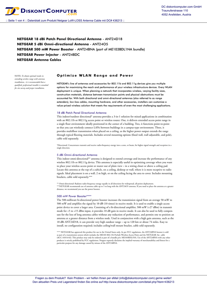
Dc Diskontcomputer Com Gmbh Traunuferstrasse 110 4052 Ansfelden Austria Manualzz
Datenblatt Samsung Galaxy Note 10 1 14 Edition Android Hilfe De
Www Infineon Com Dgdl Infineon Kp219n3621 Ds V01 00 En Pdf Fileid Db3ab5786da012b57a13ed

Infinix Note 4 Technische Daten Test Review Vergleich Phonesdata
Absolute Maximum Ratings Pin Configuration Note 1 Order Information Part Marking Package Msl Temperature Range Part Number Datasheet Ltm4639 Analog Devices

Xiaomi Redmi Note 4 Mit Vertrag Stand Januar 21 Handyhase De
Www Microchip Com Mymicrochip Filehandler Aspx Ddocname En5480

Samsung Galaxy Note 4 Wikipedia

Samsung Galaxy Note 4 Eigenschaften Technische Daten Und Preis Look4mobile
Samsung Galaxy Note 9 Preis Test Computer Bild
Datasheets Maximintegrated Com En Ds Max Pdf

Thinking Of Changing My Iphone 4 To Samsung Galaxy Note 2 Galaxy Note Samsung Note

Xiaomi Redmi Note 4 Smartphone 32gb 5 5 Grau Amazon De Elektronik
Www Intel Com Content Dam Www Programmable Us En Pdfs Literature Ds M7000a Pdf
Samsung Galaxy Note 4 Datenblatt Alle Technischen Daten
Q Tbn And9gcql Q0y8ztk0prp9cacuzr9ukf 6wdjrkcoyjbbsqa Usqp Cau
Www Ti Com Lit Gpn Lmr

Samsung Galaxy Note 4 Technische Daten Aus Indonesien

Samsung Galaxy Note 4 Technische Daten Test News Preise

Samsung Galaxy Note 4 Technische Daten Test Review Vergleich Phonesdata

Samsung Galaxy Note 4 Release Preis Daten Test

Xiaomi Redmi Note 4 Eigenschaften Technische Daten Und Preis Look4mobile
Www Raspberrypi Org Documentation Hardware Raspberrypi m2711 Rpi Data 2711 1p0 Preliminary Pdf
Exclusive Samsung Galaxy Note 4 Specs And Price Leaked From Indonesian
Www Ti Com Lit Gpn Tl431

Infinix Note 4 Technische Daten Test Review Vergleich Phonesdata

Vdi 4407

Zynq Ultrascale Rfsoc Product Data Sheet Overview Ds8
Www Nxp Com Docs En Data Sheet Mpx5700 Pdf

Infinix Note 4 Technische Daten Und Kommentare

Xiaomi Redmi Note 4 Datenblatt Alle Technischen Daten
2

Samsung Galaxy Note 4 Im Test Samsungs Kronjuwel Nextpit
Http Resources Renishaw Com En Download Data Sheet Alsi10mg 0403 400 W Powder For Additive Manufacturing
Datenblatt
Www Rfbeam Ch Files Products 12 Downloads Datasheet K Lc6 Pdf

Xiaomi Redmi Note 4 Technische Daten Im Datenblatt

Samsung Galaxy Note 4 Datenblatt Technische Daten Im Uberblick

Samsung Galaxy Note 4 Technische Daten Und Diskussion Nextpit Forum
Absolute Maximum Ratings Note 1 Pin Configuration Order Information Http Www Linear Com Product Lt1210 Orderinfo Datasheet Lt1210 Analog Devices Revision C
Cisco 4000 Family Integrated Services Router Data Sheet Cisco

Samsung Galaxy Note 10 Datenblatt Alle Technischen Daten

Samsung Galaxy Note 4 Technische Daten Test Review Vergleich Phonesdata

Samsung Galaxy Note 4 Handy Test Chip

Potentiometer Trimmer Und Regelwiderstande Datenblatter Mouser Schweiz

Virtex Ultrascale Fpga Data Sheet Dc And Ac Switching Characteristics

Xiaomi Redmi Note 4 Technische Daten Handy Entsperren24 De Blog

Samsung Galaxy Note 4 Release Preis Daten Test

Samsung Erste Technische Daten Des Galaxy Note 4 Aufgetaucht Notebookcheck Com News
Samsung Galaxy Note 4 Technische Daten Aus Indonesien

Infinix Note 4 Technische Daten Test Review Vergleich Phonesdata
Www Analog Com Media En Technical Documentation Data Sheets a Pdf

Xiaomi Redmi Note 4 Eigenschaften Technische Daten Und Preis Look4mobile
Www Ti Com Lit Gpn Tmux1104
Www Renesas Com Document Dst 026i 01 Datasheet
1
Www Sparkfun Com Datasheets Sensors Infrared Gp2y0a02yk E Pdf

Samsung Galaxy Note 5 Release Preis Technische Daten Und Bilder

Zynq 7000 Soc Z 7007s Z 7012s Z 7014s Z 7010 Z 7015 And Z 70 Dc And Ac Switching Characteristics Data Sheet
Www Onsemi Com Pub Collateral Ncp1050 D Pdf

Xs2 Round Water Resistant Connectors M12 Threads Lineup Omron Industrial Automation
Www Onsemi Com Pub Collateral Mc10ep57 D Pdf
2
Datasheets Maximintegrated Com En Ds Max Maxa Pdf
Www Diodes Com Assets Datasheets Zxtn4004k Pdf

Samsung Galaxy Note 4 Technische Daten Test News Preise
Ptfe Heat Shrink Tubing 4 1 Elringklinger Engineered Plastics

Samsung Galaxy Note 4 Technische Daten Test News Preise

Samsung Galaxy Note 4 Im Test Computer Bild

Samsung Galaxy Note 4 Datenblatt Alle Technischen Daten
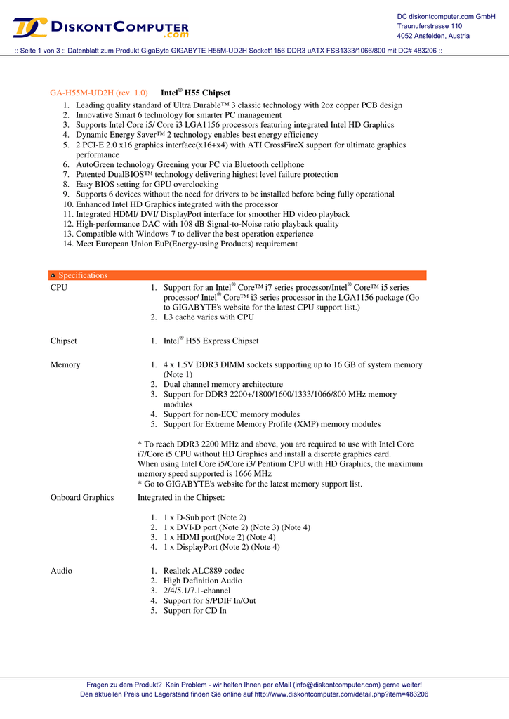
Ga H55m Ud2h Rev 1 0 Intel H55 Chipset 1 Leading Quality Manualzz
Http Www Linear Com Docs 2603

Xiaomi Redmi Note 4 Models And Versions Phonemore
Http Www Fujitsu Com Downloads Micro Fme Fram Datasheet Mb85rs64 Pdf
Philips Leaflet Released Germany German User Manual Datenblatt Pss Deude

Samsung Galaxy Note 10 Datenblatt Alle Technischen Daten
Www Tme Eu Document Af750cb7fbed26a9f817d5423 Bm71bles1fcb02aa Pdf
Www Farnell Com Datasheets Pdf

Samsung Galaxy Note 4 Im Test Computer Bild

Galaxy Note 4 Im Test Connect

Smc 2 Esd Entstorer Tvs Dioden Datenblatter Mouser Osterreich
Http Ww1 Microchip Com Downloads En Devicedoc c Pdf

Samsung Galaxy Note 4 Technische Daten Im Datenblatt

Uhans Note 4 Notebookcheck Com Externe Tests

Samsung Galaxy Note 4 Im Test Computer Bild
1 2 Ordering Information Tape And Reel Package Part Number Note 4 Part Marking Temp Range C Units Note 1 Datasheet Hip2210 Hip2211 Renesas
Xiaomi Redmi Note 4 Technische Daten Geleakt Notebookcheck Com News

Samsung Galaxy Note 4 Eigenschaften Technische Daten Und Preis Look4mobile


